Soitec has based its success story on the production of specific semiconductors (SOI) a component at the heart of advanced microelectronic devices.
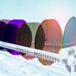
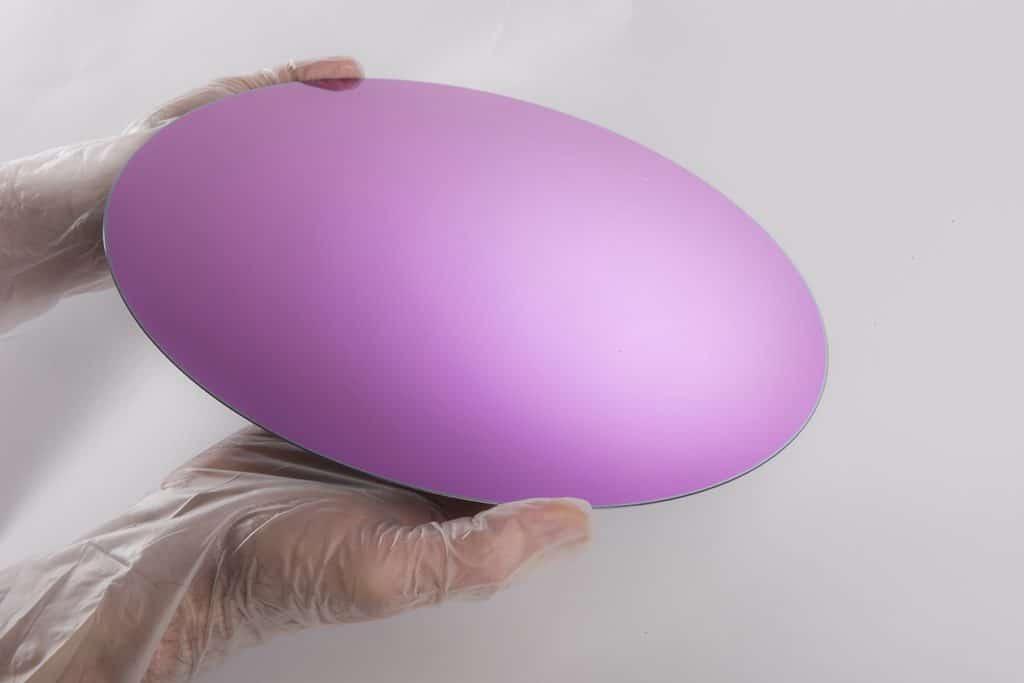
Soitec, founded in 1992 in Grenoble’s thriving high tech ecosystem, has become in less than 25 years a world leader in the design and manufacturing of innovative semiconductor materials. The company uses its advanced proprietary technology, the Smart Cut process, to produce its flagship product: silicon-on-insulator (SOI) wafers. These are used to equip advanced microelectronic devices: smartphones, computers, data centres, electronic components in cars, connected devices, industrial and medical equipment. Offering competitive solutions to miniaturize chips, improve their performance and reduce their energy usage, Soitec is helping speed up the mobile and digital revolutions.
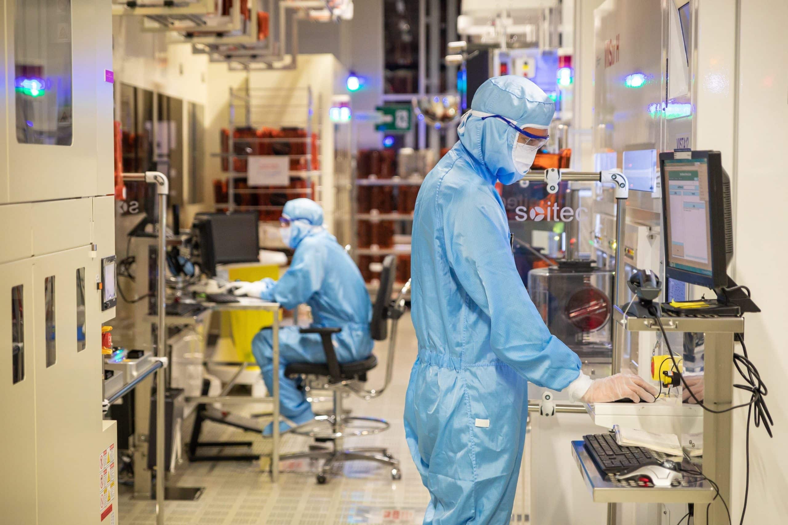
The company owns the largest manufacturing site for SOI wafers in the world. Soitec Smart Cut technology, first introduced in 1997 in the production facility of Bernin (near Grenoble) set the industry standard: it is used to make nearly all SOI wafers sold in the world today. The site is committed to sustainable development from early on, with an environmental and energy management system that makes it possible to implement continuous improvement actions like limiting atmospheric and aqueous discharges, preventing soil pollution, improving waste management, etc. Abroad, Soitec pilot line in Singapour dates back to 2008. Since 2015 the company has a manufacturing partner, Simgui, in China. Soitec generates 90% of its revenue abroad.
€444m revenue
Despite the gloomy context of the semiconductor sector, Soitec’s growth is skyrocketing. Its revenue have doubled in four years, from €222m ($244m) in 2014-2015 to €444m ($488m) in 2018-2019. The company fully benefits from the commercial deployment of 5G, the fifth generation cellular network technology, which requires the incorporation of more SOI wafers in smartphones.
Soitec also bases its growth on diversification as it significantly increases its production capacity of piezoelectric-on-insulator (POI) substrates, used for acoustic devices (sensors, filters) in order to meet growing customer demand. The coming years promise to be very busy!
