The French New Space is playing in the…
15/02/2023
27/04/2023
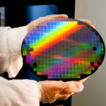
On April 18 the European Union approved the “EU Chips Act”, a €43 billion plan designed to turbocharge the European chip industry so that in ten years’ time it will account for 20% of global chip production, compared with 10% currently, and thus make Europe more independent in this sector. La French Fab is focusing on a premium positioning in the semiconductor market, supporting the EU’s aim to become, in the words of Thierry Breton, European Commissioner for the Internal Market responsible for the digital, industry and services sector, “an industrial powerhouse in the markets of the future” .
The Chips Act will support not only factory location projects but also innovation initiatives and R&D, a step forward that is welcomed by the semiconductor sector as the plan will enable the industrialization of new technologies such as the more efficient FD-SOI. The France 2030 plan will provide support for projects established on French soil.
FD-SOI: La French Fab takes the plunge
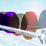
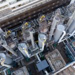
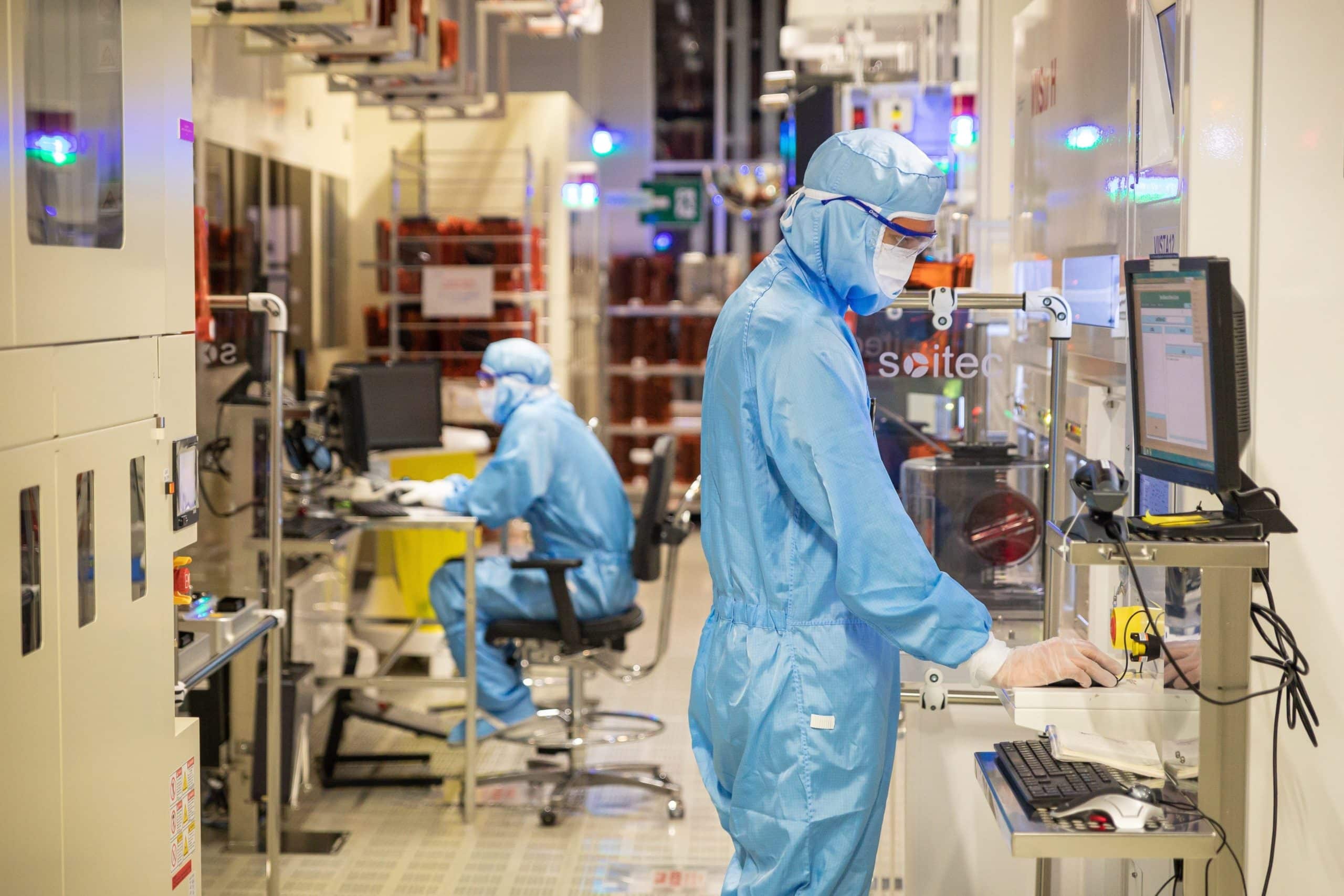
A new factory will be created in south-eastern France with the support of Franco-Italian company STMicroelectronics and US company Globalfoundries. The site will produce 28 and 22 nanometer chips on 300mm wafers, but more importantly it will make its components using FD-SOI technology (Fully Depleted-Silicon-On-Insulator) that allows significant performance and cost improvements for a variety of applications (AI, driver assistance, Internet of Things and more). R&D is already working to produce even smaller 18 and 12 nanometer chips. The factory will have access to an on-site processing unit that will recycle 50% of the water used. The site will emit 10 to 20 times less CO2 than current factories and will not release any solvents into the atmosphere. By 2026, it is expected to reach its fully operational output of 620,000 wafers a year.
Riber: French state-of-the-art quality
Miniaturization will eventually reach its physical limits, so the future for chips could take the form of breakthrough technologies such as Molecular Beam Epitaxy (MBE), a specialty of the French SME Riber that at the moment enjoys 70% of the market share in the industry. Currently reserved for specific applications such as night vision radar, this technique consists of depositing a single crystal layer of material in a vacuum, onto which components are then built. The technology is, for the moment, reserved for so-called compound semiconductors (5% of the market) but the French OEM is keen that its technology should penetrate major silicon chip plants (Intel, STMIcroelectronics and so on) and is preparing a machine designed for promising markets such as 6G, quantum or silicon photonics. Riber believes its developments will help it to achieve sales of €100 million by 2030.
Related posts:
 Semiconductors: Europe pulls it out of the bag with the Chips Act!
 Soitec, at the heart of electronics
 La French Fab leading the way in upcycling rarely recycled materials!
 STMicroelectronics: a major European player on the semiconductor market
 Start-Up France Tech in Fab
 Green hydrogen and cars: France puts the focus on giga factories
 A €2.3 billion plan to embed French industrial startups in France
 Aledia is revolutionising the display market with its led diodes
 France’s President wants startups to form the basis for 100 new industrial sites
 Technology and people at the heart of French industry
Learn more about New industrial savoir-faire
News
More news

Two French companies in the space sector have just completed…
Read more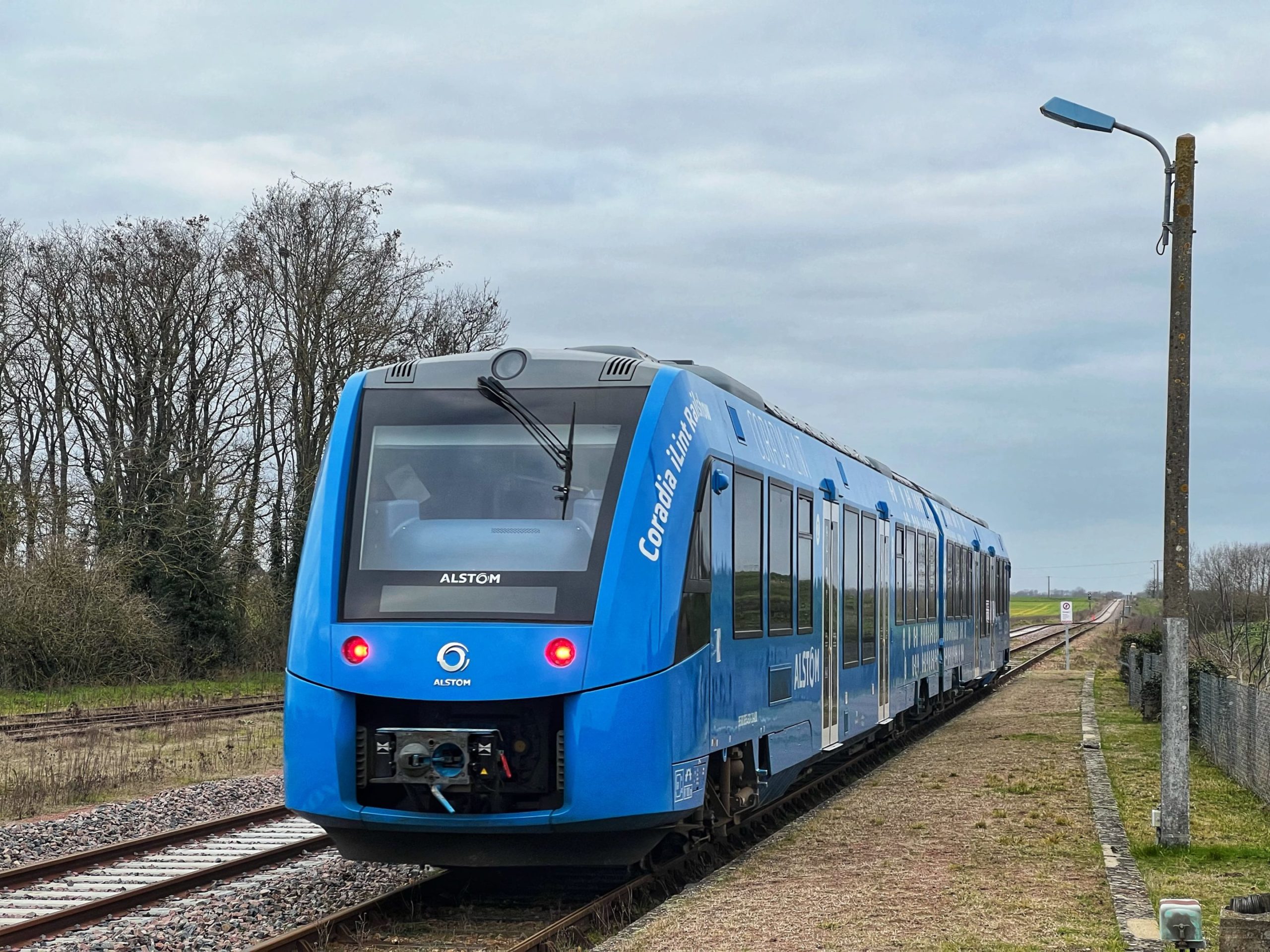
Coradia iLint, Alstom’s hydrogen train, made its first journey on…
Read more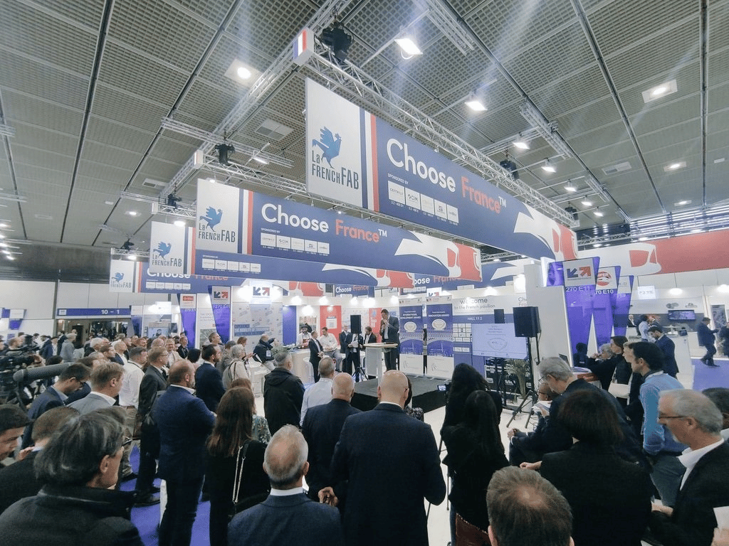
La French Fab present a wide range of large-scale international…
Read more
Airbus achieves major milestone in hydrogen-powered aircraft development and paving…
Read more
€7 billion for French deep tech and green tech companies…
Read more
La French Fab shines in the Paris Air Show where…
Read more
Soitec is investing €1 billion, half of it…
15/06/2023
French manufacturer of high-performance electronic substrates; Soitec will be investing…
Read more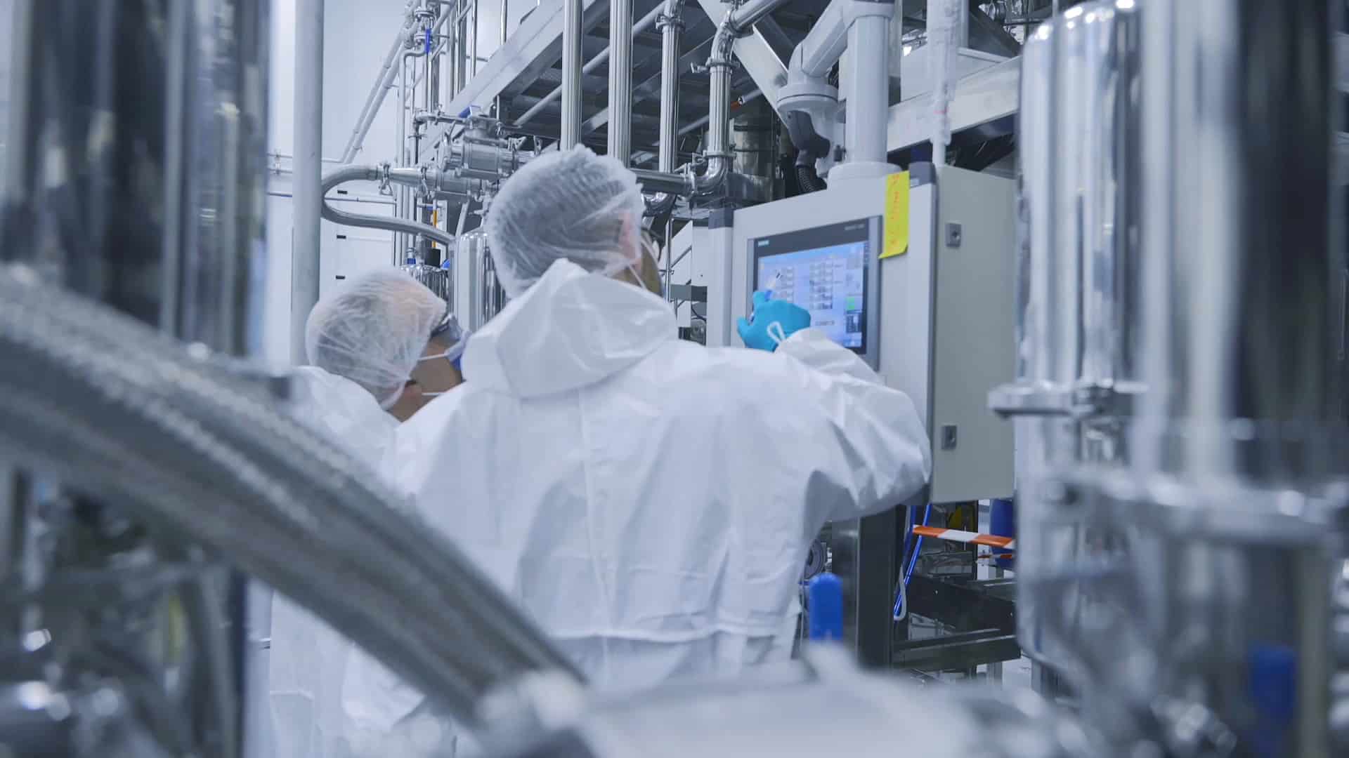
French Battery Valley operations hit the ground running with an…
Read more
The world's leading event dedicated to innovation in the automotive…
Read more
France 2030 has already set aside half of its €54…
Read more
The French parliament adopted the Nuclear Stimulus which simplifies construction…
Read more
France’s green re-industrialization enables France to position at the heart…
Read more
Inocel is industrializing its fuel cell
17/05/2023

Inocel, a startup established in 2022, has decided to step…
Read more